Time: 9:30am-11:00, (Friday) Nov.5, 2010
Venue: Room 403, R&D Building, IMR CAS
Atomic Structures and Properties of Ceramic Interfaces–Combination of Cs-corrected STEM and First Principles Calculations
Yuichi Ikuhara1,2,3
1Institute of Engineering Innovation, the University of Tokyo, Tokyo 116-0013, Japan
2Nanostructures Research Laboratory, Japan Fine Ceramics Center, Nagoya, 456-8587, Japan
3WPI Advanced Institute for Materials Research, Tohoku University, Sendai, 980-8577, Japan
Grain boundaries and interfaces of crystals have peculiar electronic structures, caused by the disorder in periodicity, providing the functional properties, which cannot be observed in a perfect crystal. In the vicinity of the grain boundaries and interfaces around the order of 1 nanometer, dopants or impurities are often segregated, and they play a crucial role in the material properties. We call these dopants “function providing elements”, which have the characteristics to change the macroscopic properties of the materials drastically. In this study, we focus our attention on grain boundaries and interfaces of various ceramics, to which “function providing elements” are doped, and introduce the latest results of the microstructure analyzed in detail by Cs-corrected STEM. The results obtained for ZnO, Al2O3, Au nanoparticles on TiO2, BTO superlattice and Li related crystals will be shown in this presentation. Furthermore, the mechanism of the “function providing elements” are analyzed by the first principles calculation based on these observation results.
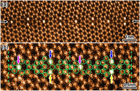
Fig.1 (a) HAADF STEM image of a Pr-doped ZnO S49 GB. Incident beam direction and GB plane are parallel to [0001] and (35 0) of both crystals, respectively. Arrows show the position of GB plane. (b) Enlarged image with the framework structure of undoped ZnO GB, which is superimposed by green circles. Dotted lines show the periodicity along the GB plane. Colored arrows indicate the location of Pr atoms, in which three different colors show three different GB atomic sites.
References
[1] Y. Ikuhara, Prog.Mater.Sci., 54 ,770-791 (2009)
[2] J.P.Buban et al., Science, 311 (5758): 212-215 (2006)
[3] N. Shibata et al,, Nature Mater., 8, 654-658 (2009)
[4] Y.Sato et al., Phys. Rev.Lett. , 97 (10): 106802 (2006)
[5] N. Shibata et al., Phys. Rev.Lett., 102(13),136105 (2009)
[6] H.Ohta et al., Nature Mater., 6 (2): 129-134 (2007)
[7] S-Y Chung et al., Phys. Rev.Lett., 100 (12): 125502 (2008)
[8]S. D. Findlay et al., APL., 95, 191913 (2009)
Yuichi Ikuhara is Professor and Director of Nanotechnology Center, Institute of Engineering Innovation at University of Tokyo since 2003. He received Dr.Eng. from Department of Materials Sciences, Kyushu University. He then joined Japan Fine Ceramics Center (JFCC) in 1988, and was the Division Manager of the Microstructure Characterization Division at JFCC from 1993. In 1996, he joined University of Tokyo as an associate professor of Materials Sciences. He was a visiting assistant professor at Case Western Reserve University from 1991 to 1993. His current research interest is in interface and grain boundary phenomena, transmission electron microscopy (STEM, HREM, EDS, EELS), high-temperature ceramics, electroceramics, dislocations, bicrystal experiments, theoretical calculations, quantum device and so on. Dr.Ikuhara is author and coauthor of 410 technical papers in the field, and has more than 200 invited talks at international and domestic conferences. He has received “Humboldt Research Award” from Alexander von Humboldt Foundation (2010), “Honda Frontier Prize” from Honda Foundation (2010), “Seto Prize” from Microscopy Society of Japan (2007), “Fulrath Award (Academic)” from the American Ceramics Society (2002), “Academic Prize” from the Ceramics Society of Japan (2001), “Exploits Awards” from the Japan Institute of Metals (2001) and so on. He is the former chief editor of “Journal of Ceramics Society”, an editorial board of “Materials Science and Engineering A”, “Materials Transaction” and so on. He is a member of the board of directors at Microscopy Society of Japan, Japan Institute of Metals, MRS of Japan and the Ceramics Society of Japan, and an associate member of the Science Council of Japan. He holds a group leader position at JFCC and WPI professor at Tohoku University concurrently.
Yuichi Ikuhara教授毕业于日本九州大学并荣获博士学位。曾任日本精细陶瓷研究中心微结构分析部主任。1996年至今Ikuhara教授任日本东京大学副教授和教授。2005年至今为东京大学工学部创新工程研究所所长。Ikuhara教授多年来主要从事透射电子显微学研究,在陶瓷材料界面结构方面具有很高的造诣。2005年Ikuhara教授与日本电子公司在东京大学成立电子显微学联合实验室,并将像差矫正技术(尤其是环型明场成像技术)成功地应用于材料精细结构的研究。他曾在国际/国内学术会议上作邀请报告200余次,在国际/国内学术刊物上发表论文400余篇。近年来在Science上发学术表论文4篇,在Nature Materials上发表论文3篇。Ikuhara教授曾荣获美国陶瓷学会Ross Coffin Purdy奖及Fulrath奖,美国微束分析学会Cosslett奖,德国“洪堡”奖,日本材料学会、日本电镜学会以及日本陶瓷学会等10多项奖项和荣誉。