Topic: Frontiers in Nanostructured Materials for Next-generation Nanotechnology
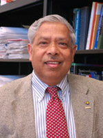
Speaker: Prof. Jagdish (Jay) Narayan
Department of Material Science and Engineering
North Carolina State University,USA
Abstract:
This lecture starts with the discussion of inherent advantages and challenges of nanoscience and nanomaterials leading to novel and unique systems with improved properties. The primary focus of this presentation is on processing control at the atomic scale, directed and controlled self-assembly processing of novel nanomaterials, nanoscale characterization and modeling to transition basic science into systems and manufacturing. The systems of interest relate to superhard materials for advanced tools in high-speed machining; novel assembled magnetic materials, nanomagnetics, spintronics, light-emitting diodes, smart integrated sensors and nanoelectronics.
We have designed novel metal-metal (where one metal component acts as diffusion barrier) and metal-ceramic nanocomposites, which have both high strength and good ductility. Controlled nanostructures in the form of nanodots and nanolayers for a variety of applications ranging from nanomagnetics and information storage to fuel efficiency and environmental protection are needed. For nanodots, we need to control their structure, composition, location, size distribution and orientation. This has been achieved by self-assembly processing on substrates which have varying degree of lattice misfit. The epitaxial orientation for nanodots and nanolayers with misfit across the scale has been achieved by using the paradigm of domain matching epitaxy. The domain matching epitaxy involves matching of integral multiples of lattice planes across the film-substrate interface, where the misfit in between the integral multiples is accommodated by the principle of domain variation, by which full lattice relaxation can be achieved at the temperature thin film growth or processing. The nanodot as well as nanolayered structures can be integrated epitaxially with Si(100) substrates by addressing epitaxy across the misfit scale via DME. The next challenge is to control defects and interfaces and correlate with the properties of nanostructures. We also cover briefly emerging nanotechnology solutions to solve energy and environmental problems by improving automobile efficiency and reducing carbon footprint and greenhouse gas emissions.
 CV-Prof. Jagdish (Jay) Narayan
Biography:
Professor Jagdish Narayan holds The John C.C. Fan Family Distinguished Chair Professorship and is Director of the NSF Center for Advanced Materials and Smart Structures at North Carolina State University. He also has the appointment of Distinguished Visiting Scientist at Oak Ridge National Laboratory.
Professor Narayan received his M.S. (1970) and Ph. D. (1971) degrees from the University of California, Berkeley, after his Bachelor’s of Technology with Distinction and Highest Honors from IIT Kanpur in 1969. Professor Narayan has had a profound impact on our understanding of defects and interfaces in thin film heterostructures, laser-solid interactions and processing of novel materials, controlled thin film growth and self-assembled nanostructures, and nanoscale characterization and modeling of new materials and properties. He pioneered the concept of solute trapping in semiconductors by his discoveries of laser annealing in the late seventies and the formation of supersaturated semiconductor alloys for which he received 1981 US-DOE Award and 1983 IR-100 on Supersaturated Semiconductor Alloys that form the backbone of modern Integrated Circuits. This research, featured twice in Science Magazine, has resulted in numerous U.S. patents and three IR-100 Awards. Professor Narayan received the 2011 Acta Materialia Gold Medal for these pioneering contributions and his leadership in materials science worldwide. The concept of solute trapping, which was introduced by John Cahn, a professor at MIT, in the early seventies, resulted in the 2011 Kyoto Prize for Cahn and the 2011 Nobel Prize for Dan Shechtman for his work on quasicrystals which formed due to solute trapping in aluminum-manganese alloys. More recently, Professor Narayan has pioneered and patented a new concept of domain epitaxy, where an integral number of lattice planes of the film match that of the substrate in large lattice mismatched systems. The domain epitaxy is key to the formation of thin film heterostructures with lattice misfits across the scale. Narayan invented new cubic ZnMgO alloys, which can be grown epitaxially on silicon (100) substrates for integrating optoelectronic and spintronics devices. He discovered and patented a new method of self-assembly for processing nanostructured magnetic, photonic, electronic, and structural materials. His discoveries related to domain epitaxy and quantum confinement by thickness variation (creating nanopockets) are being used by Kopin Corp. to manufacture high efficiency light emitting diodes for solid-state lighting.
Professor Narayan has published over 500 Journal articles, edited 9 books, and received 39 patents pertaining to novel materials and processing methods, domain epitaxy, and a new class of next-generation semiconductor alloys. He has received many honors, including 2011 Acta Mareialia Gold Medal and Prize for pioneering contributions and leadership in materials science worldwide; 2011 MRS Forum on Frontiers of Thin Film Epitaxy and Nanostructured Materials and 2011 MS&T International Symposium, honoring Narayan; 2011-12 Holladay Medal Prize, highest NCSU honor; 2011 Reynolds Prize, highest NCSU-COE honor for excellence in research, teaching and professional accomplishments; ASM Gold Medal; ASM Edward DeMille Campbell Lecture and Prize; US-DOE Outstanding Research Award; Three IR-100 Awards; Inaugural MRS Fellow (First 34 MRS members worldwide); TMS Fellow (limit 100 members worldwide); National Academy of Sciences (India) Fellow; APS Fellow, AAAS Fellow, ASM Fellow, MRS-I Honorary Member, Fellow BPS, Germany; He received Distinguished Alumnus Honors from IIT/K in 1997 along with Mr. Narayana Murthy.


